I designed my PCB at Disneyland!
Steve Ranta
I work as a field applications engineer (FAE) for Analog Devices. I had a pretty large sales opportunity at a significant customer who was working on the next revision of an existing test and measurement product. The customer was moving quickly on the design and was trying to reuse as many circuits as possible from the previous product.
Unfortunately for ADI, our ICs were not utilized in the section of the circuit being reused in the new design. Although the customer thought ADI had great IC solutions for their application needs, the engineer was not able to risk development time to layout a new PCB to evaluate the ADI solutions for the application.
I then asked the engineer if he would consider and evaluate an ADI approach if we put together a customized demo board for them. The engineer agreed to evaluate us but indicated that he would need the demo board very soon since they were locking down their schematic in a few weeks.
I had to move quickly on developing a custom demo PCB. Unfortunately for me, I was about to leave on vacation for a week to Disneyland in California with my family and I did not have a lot of time to get this demo board done. To have a chance to win this new business, I was going to have to design this PCB over my vacation.
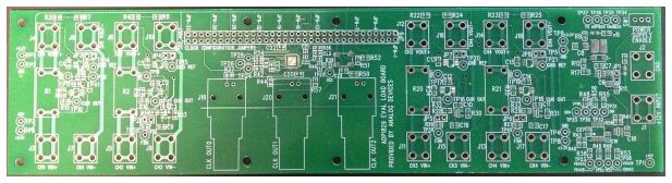
I took my laptop with me and on the airplane and in my hotel room at Disneyland, I cranked out a PCB design over a few evenings after spending the days in the parks. Once finished, I uploaded my files to Sunstone over the hotel’s wireless connection for a quick-turn fab. When I returned home a few days later, my finished PCB was waiting there, ready to populate with components!
In the end, I was able to deliver a working custom demo board in time for evaluation and the customer was very impressed with ADI for the turnaround time. We ended up winning new business over our competition and I couldn’t have done it without the quick turn-around from Sunstone!
- Shared October 10, 2012