Mr.
DonS
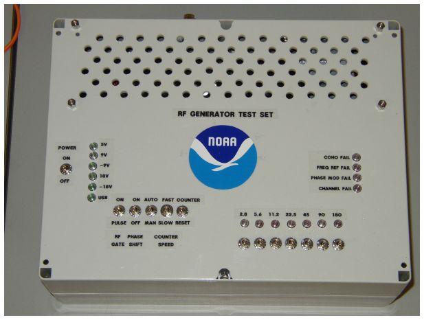
My first PCB design was an in-house built RF generator test set for the NEXRAD doppler weather radar system. I selected the enclosure and designed the arrangement of switches and LEDs for the user interface. The toggle switches and LEDs were to be soldered directly to the board and inserted up through holes in the top of the enclosure. I was at a loss for how to drill the holes in the enclosure to precisely align with the parts. Then I discovered I could edit the part in the EAGLE PCB CAD library to add a tiny hole in the center of each switch and LED footprint where the mounting hole should be centered. This created a little confusion with Sunstone when they received the Gerber files, but their folks quickly understood what I was doing. When I received the boards, I placed an unpopulated board on top of each enclosure, and used the extra holes to mark the drill spot for each part. After we populated the boards, and drilled the holes in the enclosure, the parts all aligned exactly!
- Shared December 7, 2012